


- sales/support
Google Chat:---
- sales
+86-0755-88291180
- sales01
sales@spotpear.com
- sales02
dragon_manager@163.com
- support
tech-support@spotpear.com
- CEO-Complaints
zhoujie@spotpear.com
- Only Tech-Support
WhatsApp:13246739196
- Purchase/Shipping/Refund
WhatsApp:13424403025
- HOME
- >
- ARTICLES
- >
- Common Moudle
- >
- LCD
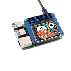
Raspberry Pi OLED/LCD HAT (A) User Guide
Overview
Introduction
The OLED/LCD HAT (A) features a 2inch IPS LCD Main Screen with built-in ST7789VW driver chip, SPI interface communication, wide viewing angle, supports 262K color display, 240×320 resolution. Dual 0.96inch OLED secondary screens with built-in SSD1315 driver chip, I2C interface communication, blue display color, 128×64 resolution, can be used to display key informations, status indicator messages or small graphics.
Comes with online development resources and manual, demos for Raspberry Pi (WiringPi library and Python demo), STM32 and Arduino.
Parameters
| Parameter Name | Parameters | |
| Power Supply | 3.3V | |
| Operating Current | 840mA | |
| Dimensions | 65.00 x 56.00(mm) | |
| Screen | 0.96inch OLED | 2inch IPS |
| Driver | SSD1315 | ST7789 |
| Communication Interface | I2C | 4-wire SPI |
| Resolution | 128 × 64 | 240 × 320 |
| Display Size | 21.74mm × 11.20mm | 30.60mm × 40.80mm |
| Pixel Size | 0.15mm × 0.15mm | 0.0975mm× 0.0975mm |
Pins
| Pins | Board |
| VCC | 3.3V |
| GND | GND |
| MOSI | 19 |
| SCLK | 23 |
| CS | 24 |
| DC | 15 |
| RST | 13 |
| SDA | 3 |
| SCL | 5 |
| KEY1 | 7 |
| KEY2 | 11 |
| KEY3 | 16 |
| KEY4 | 18 |
Hardware Description
Communication Protocol
- SPI communication protocol
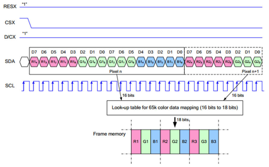
From the above, we know that 4-wire SPI communication is used, and we can get the following communication timing diagram by checking the datasheet to transmit RGB556 as an example:
Note: Different from the traditional SPI protocol, the data line sent from the slave to the master is hidden since the device only has a display requirement.
- RESX is the reset pin, it should be pulled low when powering the module and set to 1 at other times.
- CSX is slave chip select, when CS is low, the chip is enabled.
- D/CX is data/command control pin, when DC = 0, write command; when DC = 1, write data.
- SDA is the data pin for transmitting RGB data, it works as the MOSI pin of the SPI interface;
- SCL is the SPI communication clock, it works as the SCLK pins of the SPI interface.
- SPI communication has data transfer timing, which is a combination of CPHA and CPOL.
- The level of CPHA determines whether data is collected at the first clock edge or at the second clock edge of the serial synchronous clock; when CPHL = 0, data is collected at the first clock edge.
- The level of CPOL determines the level of the serial synchronous clock at an idle state. When CPOL = 0, the level is Low. However, CPOL has little effect on the transmission.
- As can be seen from the figure, when the first falling edge of SCLK starts transmitting data, a clock cycle to transmit 8-bit data, the use of SPI0, bit-by-bit transmission, the high bit in the front, the low bit in the back.
- RESX is the reset pin, it should be pulled low when powering the module and set to 1 at other times.
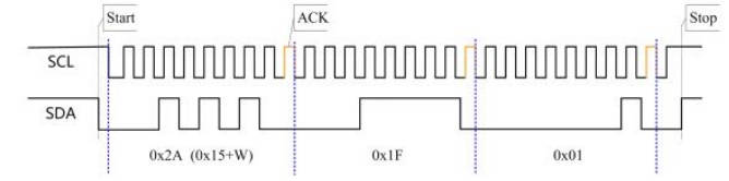
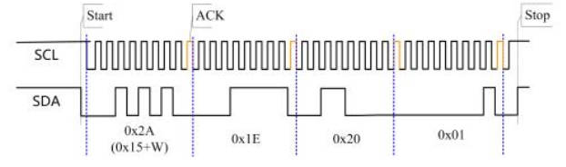
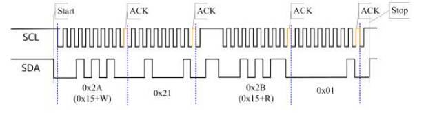
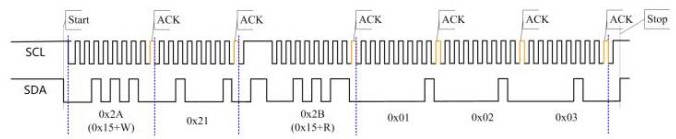
- I2C communication protocol:
The 7-bit device addresses of the SSD1315 chip are conveniently 0x1E and 0x1F, that is, the device write addresses are 0x3C and 0x3D, and the read addresses are 0x3D and 0x3E.
- Waveform Description:
Working with Raspberry Pi
Enable SPI interface
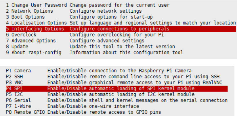
- Open the terminal, and use the command to enter the configuration page.
sudo raspi-config
Choose Interfacing Options -> SPI -> Yes to enable the SPI interface
sudo reboot
Make sure that the SPI is not occupied by other devices, you can check in the middle of the /boot/config .txt.
For I2C, enter the configuration interface and select Interface Options -> I2C -> Yes to enable the IIC interface, and then reboot.
Install Library
If you use bookworm system, only the lgpio library is available, bcm2835 and wiringPi libarary cannot be installed or used. Please note that the python library does not need to install, you can directly run the demo.
BCM2835
#Open the Raspberry Pi terminal and run the following command
wget http://www.airspayce.com/mikem/bcm2835/bcm2835-1.71.tar.gz
tar zxvf bcm2835-1.71.tar.gz
cd bcm2835-1.71/
sudo ./configure && sudo make && sudo make check && sudo make install
# For more, you can refer to the official website at: http://www.airspayce.com/mikem/bcm2835/
WiringPi
#Open the Raspberry Pi terminal and run the following command
cd
sudo apt-get install wiringpi
#For Raspberry Pi systems after May 2019 (earlier than that can be executed without), an upgrade may be required:
wget https://project-downloads.drogon.net/wiringpi-latest.deb
sudo dpkg -i wiringpi-latest.deb
gpio -v
# Run gpio -v and version 2.52 will appear, if it doesn't it means there was an installation error

# Bullseye branch system using the following command:
git clone https://github.com/WiringPi/WiringPi
cd WiringPi
. /build
gpio -v
# Run gpio -v and version 2.70 will appear, if it doesn't it means there was an installation error
lgpio
#Open the Raspberry Pi terminal and run the following command
wget https://github.com/joan2937/lg/archive/master.zip
unzip master.zip
cd lg-master
sudo make install
#Raspberry Pi 5
sudo apt install python3-rpi-lgpio
#For more details, you can refer to https://github.com/gpiozero/lg
Python
#python2
sudo apt-get update
sudo apt-get install python-pip
sudo apt-get install python-pil
sudo apt-get install python-numpy
sudo pip install RPi.GPIO
sudo pip install spidev
#python3
sudo apt-get update
sudo apt-get install python3-pip
sudo apt-get install python3-pil
sudo apt-get install python3-numpy
sudo apt-get install luma.oled -y
sudo apt install ttf-mscorefonts-installer -y
Download Test Demo
Open the Raspberry Pi terminal and run the following:
sudo apt-get install unzip -y
sudo wget https://files.waveshare.com/wiki/OLED-LCD-HAT-A/OLED_LCD_HAT_A_Demo.zip
sudo unzip ./OLED_LCD_HAT_A_Demo.zip
cd OLED_LCD_HAT_A_Demo
Run Test Demo
The following commands should be run on the Raspberry Pi, otherwise, the directory can not be indexed. (BCM2835 library is not used in this demo).
C
- Recompile and it may take a few seconds:
cd c
sudo make clean
sudo make -j 8
- Run the example demo:
# Run the 0.96-inch screen respectively:
sudo ./main 0.96

#Run the 2-inch screen respectively:
sudo ./main 2

#Run the 0.96-inch screen and 2-inch screen:
sudo ./main all

#Run the key demo:
sudo ./main key
Python
- Run two 0.96 inch screens at the same time:
sudo python double_ssd1306_128x64.py
- Run the 0.96 inch screen at address 0x3C alone:
sudo python ssd1306_oled_128x64_0x3C.py
- Run the 0.96-inch screen at address 0x3D alone:
sudo python ssd1306_oled_128x64_0x3D.py
- The 0.96 screen at address 0x3C runs the Raspberry Pi status detection program (CPU usage, CPU temperature, memory usage, disk usage):
sudo python computer_status_oled_0x3C.py
- The 0.96 screen at address 0x3D runs the key program, and the program will exit after pressing K4:
sudo python check_key_oled_0x3D.py
- The program for detecting the four buttons on the side of the command line
sudo python instruct_key.py
- key_definition.py is the program for defining the buttons
FPCP Porting
For Bullseye System
Download Drivers
Open the Raspberry Pi terminal and execute:
sudo apt-get install unzip -y
sudo apt-get install cmake -y
sudo wget https://files.waveshare.com/wiki/OLED-LCD-HAT-A/OLED_LCD_HAT_A.zip
sudo unzip ./OLED_LCD_HAT_A.zip
sudo cp OLED_LCD_HAT_A.dtbo /boot/overlays/
sudo wget https://files.waveshare.com/wiki/OLED-LCD-HAT-A/Rpi-fbcp.zip
sudo unzip ./Rpi-fbcp.zip
cd rpi-fbcp/
sudo mkdir build
cd build
sudo cmake ..
sudo make -j8
sudo install fbcp /usr/local/bin/fbcp
sudo ./fbcp
Edit the config.txt file:
sudo nano /boot/config.txt
Please block the following sentence:
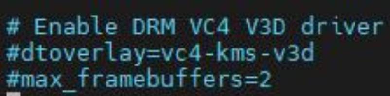
Add the following code at the end of config.txt:
dtparam=spi=on
dtoverlay=OLED_LCD_HAT_A

hdmi_force_hotplug=1
max_usb_current=1
hdmi_group=2
hdmi_mode=1
hdmi_mode=87
hdmi_cvt 640 480 60 6 0 0 0
hdmi_drive=2
display_rotate=0
Set up to Boot Automatically
sudo cp ~/rpi-fbcp/build/fbcp /usr/local/bin/fbcp
sudo nano /etc/rc.local
Add fbcp& in front of exit 0. Be sure to add the "&" and run it in the background, otherwise, the system may not boot.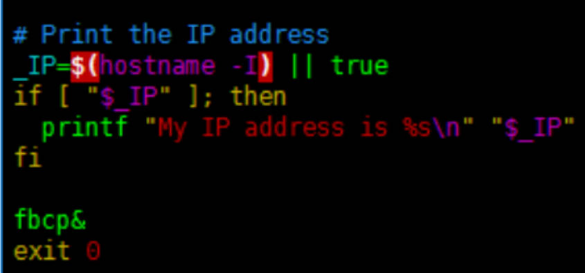
A reboot is then required:
sudo reboot
After rebooting, it can normally displays.
For Bookworm System
The operation must be based on bookworm-lite system 64-bit lite, 32-bit lite
Download Needed Software
- Update system:
sudo apt update && sudo apt upgrade && sudo apt full-upgrade -y
- Install xorg service:
sudo apt-get install --no-install-recommends xserver-xorg -y
sudo apt-get install --no-install-recommends xinit -y
- Install Desktop Manager:
sudo apt install lightdm -y
- Install Raspberry Pi official GUI:
sudo apt install raspberrypi-ui-mods -y
- Install browser (optional):
sudo apt install chromium-browser -y
Download Driver
Open the Raspberry Pi terminal and execute:
sudo apt-get install unzip -y
sudo apt-get install cmake -y
sudo wget https://files.waveshare.com/wiki/OLED-LCD-HAT-A/OLED_LCD_HAT_A.zip
sudo unzip ./OLED_LCD_HAT_A.zip
sudo cp OLED_LCD_HAT_A.dtbo /boot/overlays/
sudo wget https://files.waveshare.com/wiki/OLED-LCD-HAT-A/Rpi-fbcp.zip
sudo unzip ./Rpi-fbcp.zip
cd rpi-fbcp/
sudo rm -rf build
sudo mkdir build
cd build
sudo cmake ..
sudo make
sudo install fbcp /usr/local/bin/fbcp
Edit config.txt file:
sudo nano /boot/config.txt
Block the following sentences:
Add the following codes at the end of "config.txt":
dtparam=spi=on
dtoverlay=OLED_LCD_HAT_A:rotate=90
hdmi_force_hotplug=1
max_usb_current=1
hdmi_group=2
hdmi_mode=87
hdmi_cvt 640 480 60 6 0 0 0
hdmi_drive=2
display_rotate=0
Set Auto-start startx and fbcp
- Open ".bash_profile". If there is not ".bash_profile" file, you can create one:
sudo nano ~/.bash_profile
Add the following code at the bottom of ".bash_profile" file:
if [ "$(cat /proc/device-tree/model | cut -d ' ' -f 3)" = "5" ]; then
    # rpi 5B configuration
    export FRAMEBUFFER=/dev/fb1
    startx  2> /tmp/xorg_errors
else
    # Non-pi5 configuration
    export FRAMEBUFFER=/dev/fb0
    fbcp &
    startx  2> /tmp/xorg_errors
fi
- Open the "99-fbturbo.~" file, if it exists, you need to check fb is "fb0":
sudo nano /usr/share/X11/xorg.conf.d/99-fbturbo.~
Add the following code in "99-fbturbo.~" file:
Section "Device"
        Identifier      "Allwinner A10/A13 FBDEV"
        Driver          "fbturbo"
        Option          "fbdev" "/dev/fb0"

        Option          "SwapbuffersWait" "true"
EndSection
Set CLI Auto-login
sudo raspi-config nonint do_boot_behaviour B2
sudo raspi-config nonint do_wayland W1
sudo reboot
After rebooting, the main screen can normally display.
Note 1: Please ensure the username of the Raspberry Pi is "pi", otherwise, it cannot automatically log in.
Note 2: After setting the above configuration, it may take a while to reboot the system and load SSH.
API (Please choose C/Python to read)
Raspberry Pi series can all share a common set of programs as they are embedded systems with better compatibility.
The demo is divided into the bottom hardware interface, the middle layer LCD driver, and the upper layer application.
C
Bottom Hardware Interface
We have carried out the low-level encapsulation, if you need to know the internal implementation can go to the corresponding directory to check, for the reason that the hardware platform and the internal implementation are different. You can open DEV_Config.c(.h) to see definitions, which are in the directory RaspberryPi\c\lib\Config.
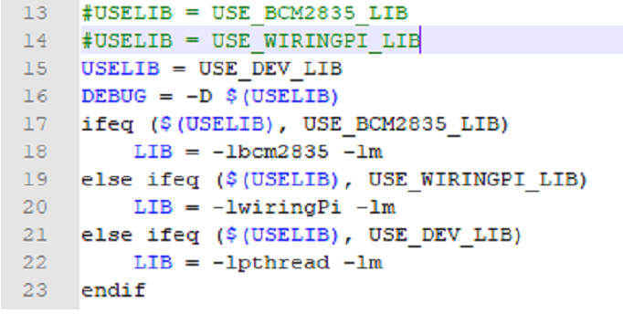
1. There are three ways for C to drive: BCM2835 library, WiringPi library, and Dev library respectively
2. We use Dev libraries by default. If you need to change to  BCM2835 or WiringPi libraries, please open RaspberryPi\c\Makefile and modify lines 13-15 as follows:
- Data type:
#define UBYTE      uint8_t
#define UWORD      uint16_t
#define UDOUBLE    uint32_t
- Module initialization and exit processing.
UBYTE DEV_ModuleInit(void);
void  DEV_ModuleExit(void);
Note:
  Here is some GPIO processing before and after using the LCD screen.
- GPIO read and write:
void 	DEV_Digital_Write(UWORD Pin, UBYTE Value);
UBYTE 	DEV_Digital_Read(UWORD Pin);
- SPI writes data:
void DEV_SPI_WriteByte(UBYTE Value);
Upper Application
If you need to draw pictures, display Chinese and English characters, display pictures, etc., we provide some basic functions here about some graphics processing in the directory RaspberryPi\c\lib\GUI\GUI_Paint.c(.h).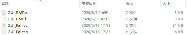
The fonts can be found in RaspberryPi\c\lib\Fonts directory.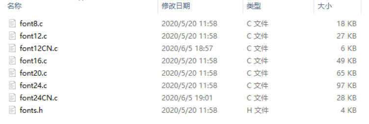
- New Image Attribute: Create a new image attribute including the name of the image cache, width, height, flip angle and color.
void Paint_NewImage(UBYTE *image, UWORD Width, UWORD Height, UWORD Rotate, UWORD Color)
Parameters:
 	   image: the name of the image cache, which is actually a pointer to the first address of the image cache;
 	   Width: the width of the image cache;
 	   Height: the height of the image cache;
 	   Rotate: the flipping angle of the image;
 	   Color: the initial color of the image;
- Select Image Cache: Select Image Cache for creating multiple image attributes, there can be multiple image cache, you can select each image you create.
void Paint_SelectImage(UBYTE *image)
Parameters:
 	   image: the name of the image cache, which is actually a pointer to the first address of the image cache;
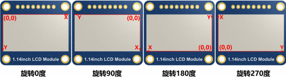
- Image rotation: set the rotation angle of the selected image. It is recommended to use it after Paint_SelectImage(), and you can choose to rotate 0, 90, 180, or 270 degrees.
void Paint_SetRotate(UWORD Rotate)
Parameters:
 	   Rotate: the rotation angle of the selected image. You can choose ROTATE_0, ROTATE_90, ROTATE_180, and ROTATE_270 corresponding to 0, 90, 180 and 270 degrees.
[Note] Under different selection angles, the coordinates correspond to different starting pixel points. Here take 1.14 as an example, four pictures in the order of 0 °, 90 °, 180 ° and 270 °for reference:
- Image mirror flip: Set the mirror flip of the selected image. You can choose no mirror, horizontal mirror, vertical mirror or image center mirror.
void Paint_SetMirroring(UBYTE mirror)
Parameters:
 	   mirror: indicates the image mirroring mode. MIRROR_NONE, MIRROR_HORIZONTAL, MIRROR_VERTICAL, MIRROR_ORIGIN correspond to no mirror, horizontal mirror, vertical mirror and image center mirror respectively.
- Set points of the display position and color in the buffer: here is the core GUI function, processing points display position and color in the buffer.
void Paint_SetPixel(UWORD Xpoint, UWORD Ypoint, UWORD Color)
Parameters:
 	   Xpoint: X position of the point in the image cache
  	   Ypoint: Y position of the point in the image cache
 	   Color: Display the point color
- Image buffer fill color: Fills the image buffer with a color, usually used to flash the screen into blank.
void Paint_Clear(UWORD Color)
Parameters:
           Color: fill color
- The fill color of a certain window in the image buffer: the image buffer part of the window filled with a certain color, usually used to fresh the screen into blank, often used for time display, fresh the last second of the screen.
void Paint_ClearWindows(UWORD Xstart, UWORD Ystart, UWORD Xend, UWORD Yend, UWORD Color)
Parameters:
           Xstart: the x-starting coordinate of the window
           Ystart: the y-starting coordinate of the window
           Xend: the x-end coordinate of the window
           Yend: the y-end coordinate of the window
           Color: fill color
- Draw point: In the image buffer, draw points on (Xpoint, Ypoint), you can choose the color, the size of the point and the style of the point.
void Paint_DrawPoint(UWORD Xpoint, UWORD Ypoint, UWORD Color, DOT_PIXEL Dot_Pixel, DOT_STYLE Dot_Style)
Parameters:
           Xpoint: indicates the X coordinate of a point.
           Ypoint: indicates the Y coordinate of a point.
           Color: fill Color
           Dot_Pixel: The size of the dot, the demo provides 8 size points by default.
                      typedef enum {
                              DOT_PIXEL_1X1  = 1,	// 1 x 1
                              DOT_PIXEL_2X2,    	// 2 X 2
                              DOT_PIXEL_3X3, 	 	// 3 X 3
                              DOT_PIXEL_4X4, 	 	// 4 X 4
                              DOT_PIXEL_5X5, 		// 5 X 5
                              DOT_PIXEL_6X6, 		// 6 X 6
                              DOT_PIXEL_7X7, 		// 7 X 7
                              DOT_PIXEL_8X8, 		// 8 X 8
               } DOT_PIXEL;
        Dot_Style: the style of a point that expands from the center of the point or from the bottom left corner of the point to the right and up.
                   typedef enum {
                     DOT_FILL_AROUND  = 1,
                     DOT_FILL_RIGHTUP,
                  } DOT_STYLE;
- Draw line: In the image buffer, draw a line from (Xstart, Ystart) to (Xend, Yend), you can choose the color, the width and the style of the line.
void Paint_DrawLine(UWORD Xstart, UWORD Ystart, UWORD Xend, UWORD Yend, UWORD Color, LINE_STYLE Line_Style, LINE_STYLE Line_Style)
Parameters:
           Xstart: the x-starting coordinate of a line
           Ystart: the y-starting coordinate of a line
           Xend: the x-end coordinate of a line
           Yend: the y-end coordinate of a line
           Color: fill color
           Line_width: The width of the line, the demo provides 8 sizes of width by default.
                 typedef enum {
                         DOT_PIXEL_1X1=1,	// 1 x 1
                         DOT_PIXEL_2X2, 	// 2 X 2
                         DOT_PIXEL_3X3,		// 3 X 3
                         DOT_PIXEL_4X4,		// 4 X 4
                         DOT_PIXEL_5X5,		// 5 X 5
                         DOT_PIXEL_6X6, 	// 6 X 6
                         DOT_PIXEL_7X7, 	// 7 X 7
                         DOT_PIXEL_8X8,		// 8 X 8
              } DOT_PIXEL;
        Line_Style: line style. Select whether the lines are joined in a straight or dashed way.
              typedef enum {
                 LINE_STYLE_SOLID = 0,
                 LINE_STYLE_DOTTED,
              } LINE_STYLE;
- Draw rectangle: In the image buffer, draw a rectangle from (Xstart, Ystart) to (Xend, Yend), you can choose the color, the width of the line and whether to fill the inside of the rectangle.
void Paint_DrawRectangle(UWORD Xstart, UWORD Ystart, UWORD Xend, UWORD Yend, UWORD Color, DOT_PIXEL Line_width, DRAW_FILL Draw_Fill)
Parameters:
	   Xstart: the starting X coordinate of the rectangle
	   Ystart: the starting Y coordinate of the rectangle
	   Xend: the x-end coordinate of the rectangle
           Yend: the y-end coordinate of the rectangle
	   Color: fill Color
	   Line_width: The width of the four sides of a rectangle. And the demo provides 8 sizes of width by default.
		     typedef enum {
			     DOT_PIXEL_1X1 = 1,	        // 1 x 1
			     DOT_PIXEL_2X2, 		// 2 X 2
			     DOT_PIXEL_3X3,		// 3 X 3
			     DOT_PIXEL_4X4,	        // 4 X 4
			     DOT_PIXEL_5X5, 		// 5 X 5
 			     DOT_PIXEL_6X6, 		// 6 X 6
                             DOT_PIXEL_7X7, 		// 7 X 7
                             DOT_PIXEL_8X8, 		// 8 X 8
                 } DOT_PIXEL;
         Draw_Fill: Fill, whether to fill the inside of the rectangle
                typedef enum {
                 	DRAW_FILL_EMPTY = 0,
                 	DRAW_FILL_FULL,
              } DRAW_FILL;
- Draw circle: In the image buffer, draw a circle with Radius as the radius and (X_Center Y_Center) as the center. You can choose the color, the width of the line and whether to fill the inside of the circle.
void Paint_DrawCircle(UWORD X_Center, UWORD Y_Center, UWORD Radius, UWORD Color, DOT_PIXEL Line_width, DRAW_FILL Draw_Fill)
Parameters:
	   X_Center: the x coordinate of the center of the circle
	   Y_Center: the y coordinate of the center of the circle
	   Radius: indicates the radius of a circle
	   Color: fill color
	   Line_width: The width of the arc, with a default of 8 widths
		typedef enum {
        		DOT_PIXEL_1X1  = 1,	// 1 x 1
        		DOT_PIXEL_2X2  , 		// 2 X 2
        		DOT_PIXEL_3X3  ,		// 3 X 3
        		DOT_PIXEL_4X4  ,		// 4 X 4
        		DOT_PIXEL_5X5  , 		// 5 X 5
        		DOT_PIXEL_6X6  , 		// 6 X 6
        		DOT_PIXEL_7X7  , 		// 7 X 7
        		DOT_PIXEL_8X8  , 		// 8 X 8
		} DOT_PIXEL;
	  Draw_Fill: fill, whether to fill the inside of the circle
               typedef enum {
              		DRAW_FILL_EMPTY = 0,
                 	DRAW_FILL_FULL,
              } DRAW_FILL;
- Write Ascii character: In the image buffer, use (Xstart, Ystart) as the left vertex, and write an Ascii character, you can select Ascii visual character library, font foreground color and font background color.
void Paint_DrawChar(UWORD Xstart, UWORD Ystart, const char Ascii_Char, sFONT* Font, UWORD Color_Foreground,  UWORD Color_Background)
Parameters:
	   Xstart: Character's left-top point X-coordinate
	   Ystart: Character's left-top point Y-coordinate
	   Ascii_Char: indicates the Ascii character
	   Font: Ascii visual character library, in the Fonts folder the demo provides the following Fonts:
  		 Font8: 5*8 font
    		 Font12: 7*12 font
    		 Font16: 11*16 font
    		 Font20: 14*20 font
    		 Font24: 17*24 font
  	  Color_Foreground: font color
  	  Color_Background: background color
- Write English string: In the image buffer, use (Xstart, Ystart) as the left-top point, and write a string of English characters, you can choose Ascii visual character library, font foreground color and font background color.
void Paint_DrawString_EN(UWORD Xstart, UWORD Ystart, const char * pString, sFONT* Font, UWORD Color_Foreground,  UWORD Color_Background)
Parameters:
	  Xstart: Character's left-top point X-coordinate
	  Ystart: Character's left-top point Y-coordinate
	  PString: string, string is a pointer
	  Font: Ascii visual character library, in the Fonts folder the demo provides the following Fonts:
     		Font8: 5*8 font
     		Font12: 7*12 font
     		Font16: 11*16 font
     		Font20: 14*20 font
     		Font24: 17*24 font
	  Color_Foreground: font color
  	  Color_Background: background color
- Write Chinese string: In the image buffer, use (Xstart, Ystart) as the left-top point, and write a string of Chinese characters, you can choose the GB2312 encoding character font, font foreground color and font background color.
void Paint_DrawString_CN(UWORD Xstart, UWORD Ystart, const char * pString, cFONT* font, UWORD Color_Foreground, UWORD Color_Background)
Parameters:
	  Xstart: Character's left-top point X-coordinate
	  Ystart: Character's left-top point Y-coordinate
	  PString: string, string is a pointer
  	  Font: GB2312 encoding character Font library, in the Fonts folder the demo provides the following Fonts:
     		Font12CN: ASCII font 11*21, Chinese font 16*21
     		Font24CN: ASCII font 24*41, Chinese font 32*41
	  Color_Foreground: font color
	  Color_Background: background color
- Write numbers: In the image buffer, use (Xstart, Ystart) as the left-top point, and write a string of numbers, you can choose Ascii visual character library, font foreground color and font background color.
void Paint_DrawNum(UWORD Xpoint, UWORD Ypoint, int32_t Nummber, sFONT* Font, UWORD Color_Foreground, UWORD Color_Background)
Parameters:
 	  Xstart: Character's left-top point X-coordinate
 	  Ystart: Character's left-top point Y-coordinate
 	  Nummber: the number displayed here is saved as a 32-bit int type, which can be displayed up to 2147483647.
 	  Font: Ascii visual character library, in the Fonts folder the demo provides the following Fonts:
 	 	font8: 5*8 font
 	 	font12: 7*12 font
 	 	font16: 11*16 font
 	 	font20: 14*20 font
 	 	font24: 17*24 font
 	Color_Foreground: font color
 	Color_Background: background color
- Write numbers with decimals: In the image buffer, use (Xstart, Ystart) as the left-top point, write a series of numbers with decimals. You can select the ASCII code visual character library, font foreground color and font background color.
void Paint_DrawFloatNum(UWORD Xpoint, UWORD Ypoint, double Nummber, UBYTE Decimal_Point, sFONT* Font, UWORD Color_Foreground, UWORD  Color_Background);
Parameters:
 	   Xstart: Character's left-top point X-coordinate
 	   Ystart: Character's left-top point Y-coordinate
 	   Nummber: Displayed numbers, here stored as double type, which are sufficient for common requirements
           Decimal_Point: Displaying digits after the decimal point
 	   Font: Ascii visual character library, in the Fonts folder the demo provides the following Fonts:
 	 	font8: 5*8 font
 	 	font12: 7*12 font
 	 	font16: 11*16 font
 	 	font20: 14*20 font
 	 	font24: 17*24 font
 	   Color_Foreground: font color
 	   Color_Background: background color
- Display time: In the image buffer, use (Xstart, Ystart) as the left-top point, display a time duration. You can choose the ASCII code visual character library, font foreground color and font background color.
void Paint_DrawTime(UWORD Xstart, UWORD Ystart, PAINT_TIME *pTime, sFONT* Font, UWORD Color_Background, UWORD Color_Foreground)
Parameters:
 	   Xstart: Character's left-top point X-coordinate
 	   Ystart: Character's left-top point Y-coordinate
 	   pTime: The displayed time is defined using a time structure. You can pass individual digits for hours, minutes and seconds as parameters;
 	   Font:  ASCII code visual character library, with the following fonts available in the Fonts folder;
 	 	font8: 5*8 font
 	 	font12: 7*12 font
 	 	font16: 11*16 font
 	 	font20: 14*20 font
 	 	font24: 17*24 font
 	   Color_Foreground: font color
 	   Color_Background: background color
- Read local bmp images and write them to a buffer.
This is possible for Raspberry Pi and other Linux-based operating systems.
For Raspberry Pi, you can refer to the directory: RaspberryPi\c\lib\GUI\GUI_BMPfile.c(.h).
UBYTE GUI_ReadBmp(const char *path, UWORD Xstart, UWORD Ystart)
Parameters:
	   path: the corresponding path of BMP pictures
 	   Xstart: The X-coordinate of the left-top point of the image, typically passed as 0 by default.
 	   Ystart: The Y-coordinate of the left-top point of the image, typically passed as 0 by default.
Python (For Raspberry Pi)
It is for Python and Python3.
For Python, its invocation are not as complicated as C.
lcdconfig.py
- Module initialization and exit processing.
def module_init()
def module_exit()
Note:
1. Here are some GPIO processing before and after using the LCD screen.
2. The module_init() function is automatically called in the init() initializer on the LCD, but the module_exit() function needs to be called by itself.
- GPIO read and write.
def  digital_write(pin, value)
def  digital_read(pin)
- SPI write data.
def spi_writebyte(data)
About Rotation Settings
If you need to set the screen rotation in the python program, you can set it by the statement im_r= image1.rotate(270).
im_r= image1.rotate(270)
- Rotation effect, take 1.14 as an example, the order is 0°, 90°, 180°, 270°.
GUI Functions
Python has an image library PIL official library link, it does not need to write code from the logical layer like C and can directly call the image library for image processing. The following will take a 1.54-inch LCD as an example, we provide a brief description of the demo.
- It needs to use the image library and install the library.
sudo apt-get install python3-pil
And then import the library:
from PIL import Image,ImageDraw,ImageFont
Among them, Image is the basic library, ImageDraw is the drawing function library, and ImageFont is the font library.
- Define an image cache to facilitate drawing, writing and other functions on the picture.
image1 = Image.new("RGB", (disp.width, disp.height), "WHITE")
The first parameter defines the color depth of the image, defined as "RGB" means RGB888 color image. The second parameter is a tuple that defines the width and height of the image. The third parameter defines the default color of the buffer, which is defined as "WHITE".
- Create a drawing object based on Image1 on which all drawing operations will be performed.
draw = ImageDraw.Draw(image1)
- Draw line.
draw.line([(20, 10),(70, 60)], fill = "RED",width = 1)
The first parameter is a 4-element tuple, with (20, 10) as the starting point and (70, 60) as the ending point, to draw a straight line. fill="RED" indicates that the line is in red color, and width=1 means that the line is 1 pixel wide.
- Draw rectangle.
draw.rectangle([(20,10),(70,60)],fill = "WHITE",outline="BLUE")
The first parameter is a 4-element tuple, with (20, 10) as the coordinates of the upper-left corner of the rectangle, and (70, 60) as the coordinates of the lower-right corner of the rectangle. fill="WHITE" specifies that the interior is filled with white color, and outline="BLUE" indicates that the outer border is blue.
- Draw circle.
draw.arc((150,15,190,55),0, 360, fill =(0,255,0)
Draw an inscribed circle in the square, the first parameter is a tuple of 4 elements, with (150, 15) as the upper left corner vertex of the square, (190, 55) as the lower right corner vertex of the square, specifying the level median line of the rectangular frame is the angle of 0 degrees, and the angle becomes larger clockwise; the second parameter indicates the starting angle; the third parameter indicates the ending angle, and fill = (0,255,0) indicates that the color of the line is green. If you are not using the square, what you draw will be an ellipse, which is a drawing of an arc.
Besides the arc function, you can also use the ellipse function for drawing a solid circle.
draw.ellipse((150,65,190,105), fill = (0,255,0))
In essence, it's drawing an ellipse. The first parameter specifies the enclosing rectangle, and fill = (0, 255, 0) indicates that the interior is filled with green color. If the the enclosing rectangle of the ellipse is a square, the ellipse becomes a circle.
- Write character.
The ImageFont module needs to be imported and instantiated:
Font1 = ImageFont.truetype("../Font/Font01.ttf",25)
Font2 = ImageFont.truetype("../Font/Font01.ttf",35)
Font3 = ImageFont.truetype("../Font/Font02.ttf",32)
You can use the fonts of Windows or other fonts which is in ttc format.
Note: Each character library contains different characters; If some characters cannot be displayed, it is recommended that you refer to the encoding set to be used. To draw English characters, you can directly use the fonts; for Chinese characters, you need to add a symbol "u":
draw.text((40, 50), 'WaveShare', fill = (128,255,128),font=Font2)
text= u"微雪电子"
draw.text((74, 150),text, fill = "WHITE",font=Font3)
The first parameter is a 2-element tuple with (40, 50) as the left-top point. The font is set to Font2, and you can specify the font color with fill. You can directly use fill = "WHITE", as standard color values are already defined. Alternatively, you can use fill = (128, 255, 128), where the values in parentheses correspond to the RGB values for precise color control.
The second line displays "微雪电子" using Font3, with the font color set to white.
- Read local pictures.
image = Image.open('../pic/LCD_1inch28.jpg')
The parameter is the image path.
- Other functions.
Python's image library is very powerful, if you need to implement more, you can learn on the website: https://pillow.readthedocs.io/en/stable/.
Resource
Document
Datasheet
Demo
Software
Pre-install image
FAQ
Question:The LCD screen is black using a Raspberry Pi for control?
a) Check if SPI (Serial Peripheral Interface) is enabled.
b) Verify if the backlight pin has output. If there is no output, you can try leaving the BL (backlight) control cable unconnected.
Question:Incorrect usage of the Raspberry Pi for control may lead to the following:
If running the wiringPi demo works normally, then running the Python or BCM2835 demo might result in the screen not refreshing properly. This is because the BCM2835 library is a library for the Raspberry Pi's CPU chip and its bottom layer is directly operating registers. The bottom layer of the wiringPi library and python operate the device by reading and writing the device file of the linux system, which may cause the GPIO port to be abnormal. Rebooting the Raspberry Pi can often provide a perfect solution.
Question:How to flip the image?
In C language, you can control rotation using the function Paint_SetRotate(Rotate). However, in C, the rotation angle can only be set to 0, 90, 180 or 270 degrees. In Python, you can call rotate(Rotate) to flip any angle.
Question:What about the Python Image library?
For some Raspberry Pi systems, the 'image' library may not be available. You can run: 'sudo apt-get install python-imaging' to install the 'python-imaging' library.
Support
Monday-Friday (9:30-6:30) Saturday (9:30-5:30)
Mobile: +86 13434470212
Email: services04@spotpear.com
[Tutorial Navigation]
- Overview
- Working with Raspberry Pi
- Download Test Demo
- Run Test Demo
- FPCP Porting
- API (Please choose C/Python to read)
- Resource
- FAQ
- Question:The LCD screen is black using a Raspberry Pi for control?
- Question:Incorrect usage of the Raspberry Pi for control may lead to the following:
- Question:How to flip the image?
- Question:What about the Python Image library?
- Support